What is a PCB Via?
A PCB via is a small hole drilling from the Fr4 sheet material, that allows electrical connections between the different copper layers. The PCB Via is lead with a conductive material, such as copper, which material allows current to go through the holes and the copper layer, then establish a connection between the copper layers. LHD PCB has a VCP copper plating line, which can make the PCB vias better and easier. The via PCBs are essential in double-layer and multi-layer PCBs as they provide a kind of electrical and thermal connection between the different copper layers of the PCBs.
Vias PCB can be drilled through the whole thickness of the PCB board, then connecting all the copper layers. Or they can be drilled some through the board, and connecting only a few copper pattern layers. LHD PCB has a VCP copper plating line, which can make the PCB vias better and easier. The size and shape of the vias depend on the function and customers’ requirements. PCB vias can be round or not, and their diameter can range from 0.1mm to 10 mm, or even more bigger. LHD PCB can produce HDI holes as small as 0.1mm, and big holes as big as 6mm, the bigger ones need to use milling way to do them.
The location of PCB vias is very important to the PCB design process. PCB vias are normally located in areas, where there are no important component modules or copper traces, as they can affect the PCB signal. LHD PCB has a VCP copper plating line, which can make the PCB vias better and easier. The location of vias can affect the board’s function, it is important to check the thermal request of the design when confirming the location of PCB vias. Kinds types of Via in PCB board.
There are many kinds types of vias in PCB board, each with its special characteristics and function.
Below are some of the most normal kinds types of vias in PCB board:
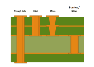
- Through hole Via:
The through hole via is the most normal type of via in the PCB board. It is a hole that extends through the whole PCB thickness of the board. And connects all the copper layers of the PCB. Through-hole PCB vias are normally used for higher current connections or for providing mechanical support to fix the board. They are also useful in applications where there is a need for a solid, continuous connection between the copper layers of the PCB. LHD PCB has rich experience in producing kinds of PCBs with through-hole vias. - Blind Via:
A blind via is a hole that connects the outer copper layer of the board to one or more inner layers, but it does not drill through the whole board. Blind vias are normally used in high-density PCB boards where space is not enough. They allow the connections between the outer copper layers of the board and the inner copper layers, without the need for the through hole which uses valuable PCB board space. LHD PCB has rich experience in producing kinds of PCB with blind via. - Buried Via:
The buried via is a kind of hole that connects two or more inner copper layers of the PCB board. However, it does not drill to the outer copper layer of the PCB board. Buried vias are useful in high-density PCB boards, where there is a need for a huge number of connections between the inner layers of the PCB boards. The buried via offers a space-saving solution that allows for more connections, which will not increase the PCB board’s size. LHD PCB has rich experience in producing kinds of PCBs with buried vias. - Via-in-pad:
The via-in-pad is a hole that is located directly under a component with a BGA pad or some other SMD pad. The Via in pad technology is useful in high-density PCB boards(HDI PCB boards), where space is very small. LHD PCB has a very good ability to produce kinds of PCB with via-in-pad. The via-in-pad allows for a more direct connection between the component and the board, reducing the length of the trace and improving the PCB signal quality. It also reduces the risk of a solder mask dam, as the via is filled with conductive or non-conductive material during the assembly process. LHD PCB has rich experience in producing kinds of PCBs via in-pad. - Micro Via:
A micro via PCB is a small diameter via that is normally less than 0.15mm. LHD PCB has rich experience in producing kinds of HDI PCBs with micro via. Micro vias are useful in HDI PCB boards where space is not enough, and there is a need for a large number of connections for each layer. LHD PCB produces the micro PCB board is also useful in high-frequency applications where signal integrity is critical. - Stacked Via for HDI PCB board:The stacked via is a via that is created by drilling two or more holes that are stacked on top of each other. These stacked via can not seen in the outer layer, and most time they are used for the HDI PCB board. Stacked vias are useful in high-density HDI PCB boards where there is a need for a large number of connections between the inner copper layers. LHD PCB has rich experience in producing kinds of HDI PCBs with stacked vias. LHD PCB produces the stacked vias which offer some space-saving solution that allows for more connections without increasing the PCB board’s size.